Introduction:
This module is the result of a request of Hans-Joachim Helmstedt, developer of the Formant MSS2000 modular synthesizer and the author of the corresponding book. He asked me to develop a module which works as easy to integrate and easy to use MIDI Arpeggiator for him:
Spec list:
- No generic MIDI processor which has to be configured
- Built as module for a modular setup
- To be integratable in any MIDI chain
- Plug in and use
- 5 different programs how MIDI chords should be serialized:
- Down-Up
- Down
- Random
- Up
- Up-Down
- Remote control / external trigger
- Transparent passing of MIDI sequences when not activated by remote control
- Adjustable processing and repetition speed (CLOCK)
- Manually with a pot
- Per CV
- Per external clock input
- Speed / clock created by the module or provided externally is provided at a clock output for synchronization purposes of other modules
- Monophonic MIDI streams are processed with a ratcheting effect, only chords are processed with arpeggio
- Ratcheting repetition rate is determined by program selecten (2-6)
First demo video: A polyphonic keyboard is used with a monophonic modular setup:
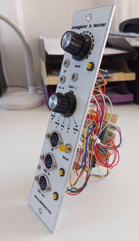
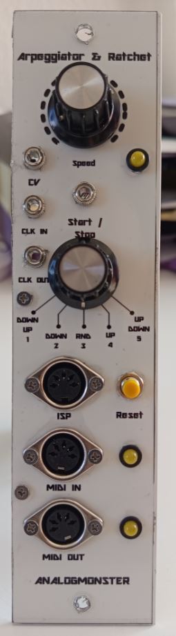
| The MIDI Arpeggiator and Ratcheting Module: | ||||
|
| |||
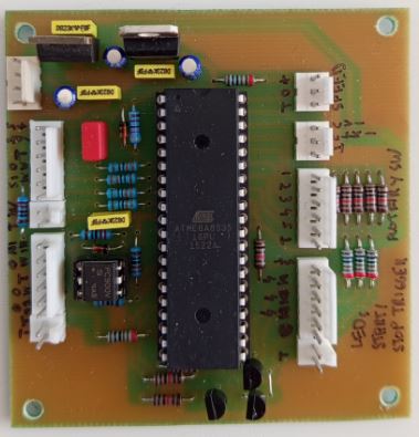
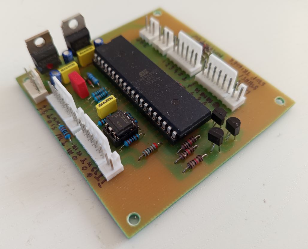
| Circuit: | Click here: KiCad schema | |||
| The circuit is built around an ATmega8535 microcontroller. | ||||
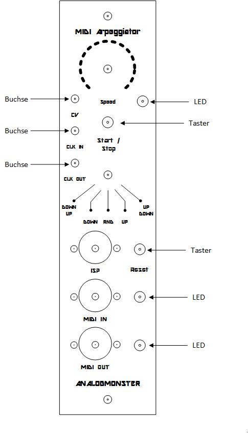
| Speed potentiometer: An adjustable voltage divider (RV1) is connected to the ADC 0 port of the microcontroller. R2 prevents a direct connection to +5V. The software reads the voltage periodically and derives the clock speed from it. | ||||
| CV input: The CV input is connected to the ADC 1 port of the microcontroller. It is scanned periodically by the software as well and influences the CLOCK speed. | ||||
| CLOCK LED: This display LED shows the ratcheting and arpeggio processing ratio (CLOCK). It is controlled by software via controller pin PD4. The pin output is amplified by R18 and Q1. The LED is placed in the collector branch of the transistor, not in the emitter branch to avoid unwanted light dimmed flashes of the LED due to the base-emitter voltage of the transistor. | ||||
| Start / Stop input: A remote control (S-Trigger) to init ratcheting or arpeggio is connected here. T2 was implemented as jack bush to be able to pull controller pin PC5 to ground by a remote cable trigger or an external S-Trigger signal. | ||||
| CLK IN: The external CLOCK input is connected to the ADC 2 port of the microcontroller. It is scanned periodically by the software as well and influences the CLOCK speed as the internal clock synchronizes with the external clock signal. | ||||
| CLK OUT: The clock output is fed by controller pin PD5 via R17. The output signal follows the internal clock. | ||||
| Program selection: This rotary switch selects the ratcheting or arpeggio program. According to the position one of the controller pins PA3 to PA7 is pulled to ground, which is scanned and interpreted by the software. The controller pins are connected to +5V via R4, R5, R6, R8 and R9. | ||||
| ISP: Din connector for firmware upload via R11 to R14 to the ISP interface pins /RESET, PB5 (MOSI), PB6 (MISO) and PB7 (SCK) | ||||
| RESET trigger: Reset mimik of the controller with T1 which discharges the capacitor C2 and therefore pulls /RESET to ground. That triggers the RESET interrupt in the controller. Via R1 the capacitor is charged over a certain time constant to ensure a certain /RESET time. As /RESET is connected externally by the ISP interface as well, D1 is implemented as protection diode. | ||||
| MIDI IN: Din connector for MIDI input. Current-loop physics. The input current goes via R7 to the opto coupler U3. There it is isolated galvanically, inverted and pulls down to ground controller pin PD0 (RXD) periodically, which is pulled up to +5V via R10. | ||||
| MIDI IN LED: This display LED shows an incoming MIDI signal. It is controlled by software via controller pin PD2. The pin output is amplified by R21 and Q3. The LED is placed in the collector branch of the transistor, not in the emitter branch to avoid unwanted light dimmed flashes of the LED due to the base-emitter voltage of the transistor. | ||||
| MIDI OUT: Din connector for MIDI output. Current-loop physics. The output current is created by PD1 (TXD) as current sink via R16. R15 at +5V serves as current source. | ||||
MIDI OUT LED: This display LED shows an outgoing MIDI signal. It is controlled by software via controller pin PD3. The pin output is amplified by R20 and Q2. The LED is placed in the collector branch of the transistor, not in the emitter branch to avoid unwanted light dimmed flashes of the LED due to the base-emitter voltage of the transistor.
|