Introduction:
As this is a keyboard synthesizer I had to build a keyboard interface obviously. Of course I wanted to implement / prepare all keyboard specials of the Syrinx (LFO 1 behavior on key strike, LFO 2 behavior on key strike, portamento), but as my synthesizer housing contains a FATAR keyboard I decided to add some addtitional stuff which the original does not provide, due to a resistor string architecture which was common in that time. Here a functional overview of my version:
- Internal CV / GATE creation: Like the Syrinx
- Internal Tune COARSE and Tune FINE adjustment: Like the Syrinx
- Portamento time adjustment: Like the Syrinx
- LFO 1 behavior on key strike: Like the Syrinx
- LFO 2 behavior on key strike: Like the Syrinx
- Portamento ON / OFF switch: New
- Key Velocity analysis: New
- Key Velocity Impact adjustment: New
- Internal Keybord or External MIDI system control selection: New
- MIDI IN OUT THRU: New
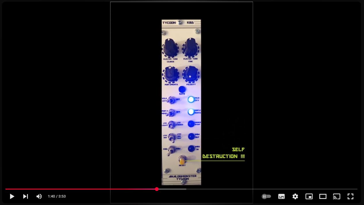
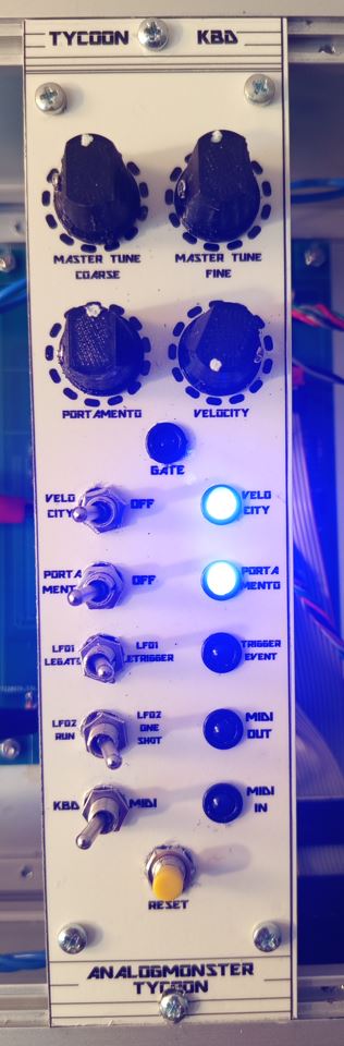
Human interface
- MASTER TUNE COARSE adjustment pot
- MASTER TUNE FINE adjustment pot
- PORTAMENTO time adjustment pot
- VELOCITY impact adjustment
Determines the derivation of the MIDI OUT note volume dependent on the key velocity. - VELOCITY switch
Activates / deactivates the key velocity analysis. The state is indicated by an LED for faster overview. - PORTAMENTO switch
Activates / deactivates the portamento function. The state is indicated by an LED for faster overview. - LFO 1 behavior selection
Will determine the behavior of LFO 1 on every key strike, meaning whether the LFO 1 is reset on every key strike to start a new wave cycle or just continues oscillating. The keyboard interface just transports the decision on the system internal bus. The LFO will have to execute it. - LED TRIGGER EVENT
Flashes on every trigger keyboard control creates. - LFO 2 behavior selection
Will determine the behavior of LFO 2 on every key strike, meaning whether the LFO 2 performs a continous run or performs only one waveform cycle. The keyboard interface just transports the decision on the system internal bus. The LFO will have to execute it. - LED MIDI OUT
Flashes on each outgoing MIDI sequence. MIDI OUT is automatically enabled on internal keyboard system control activation. - KBD MIDI system control switch
Determines whether the TyCoon is controlled by the internal keyboard or by an external MIDI stream. - LED MIDI IN
Flashes on each incoming MIDI sequence. MIDI IN is automatically enabled on external MIDI system control activation. - RESET TRIGGER
Emergency MPU reset of the keyboard interface
Circuit description
Click to open
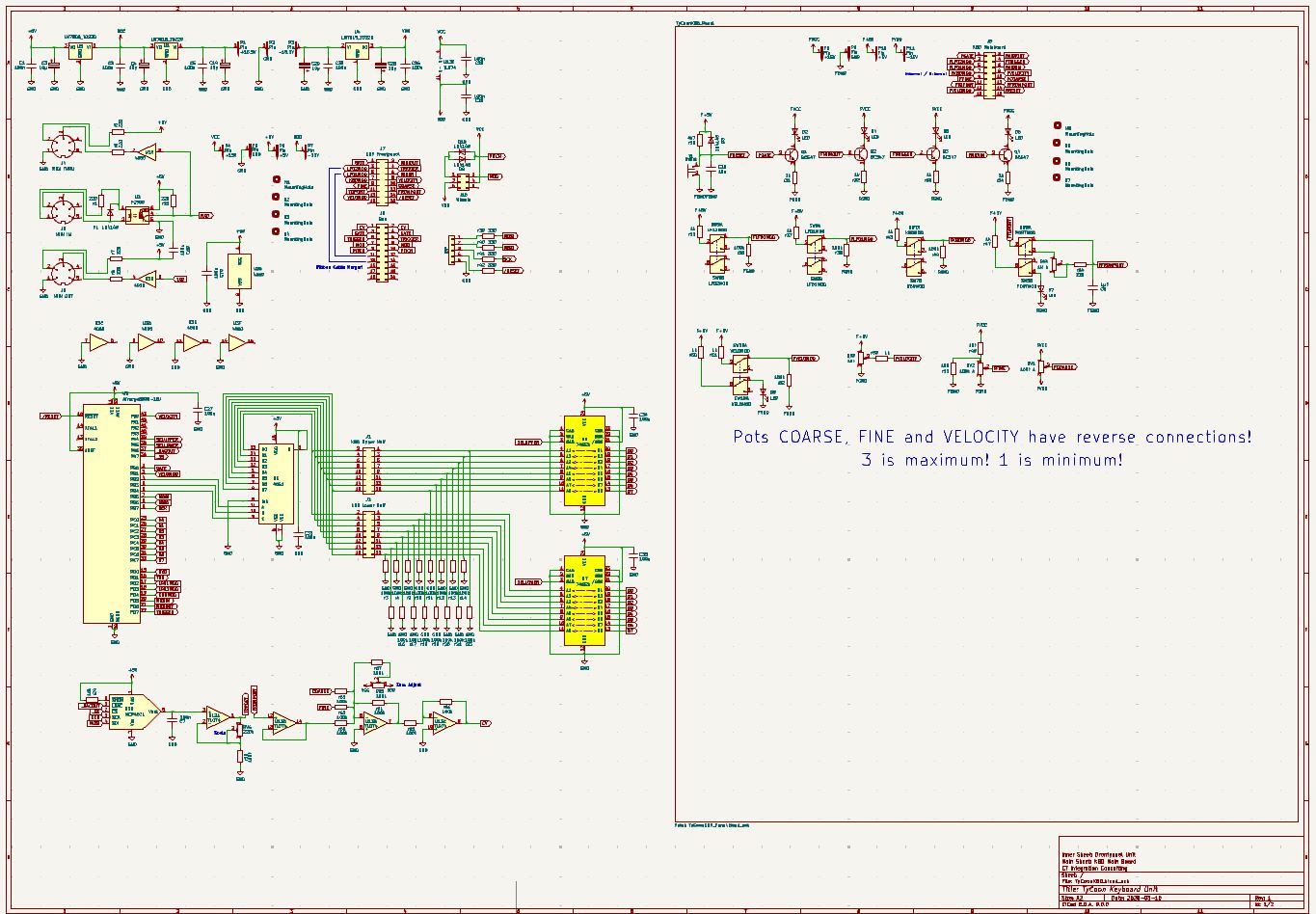
MPU
The MPU is driven by the ATmega8535 microcontroller U9. The software is uploaded by a standard ISP interface (J3, r39-r42)). The 5-pin DIN connector is located at the synthesizers back side. The controller is run by the internal 8 mhz oscillator set by fuses, so a crystal could be omitted. The /RESET circuit is located on the front panel board (see below).
The FATAR keyboard halfs are scanned by the 4051 decoder (U6) simultanously. The pressed key data of the keyboard halfs are isolated by the bus transceivers 74652 (U7, U8) which pass the data to the data bus when selected by the microcontroller (SELUPPER, SELLOWER). The FATAR output lines are pulled to ground by the 100k resistors r3,r4,r9-r14,r16-r21,r23.
The software creates the internal CV with the 12 bit DAC MCP4821 (U10), which is connected by the SPI standard to the microcontroller as slave. The CV can be normalized to 1V/octave behavior by the opamp U13A, the 220k trimmer RV6 (Scale) and the 100k resistor r59.
The CV is sent to the front panel circuit (J7) which performs the portamento handling (TOPORT, FROMPORT, voltage follower U13D). Next is an inverting DC mixer which adds the TUNE COARSE and FINE voltages together with a zero adjust. Last is another voltage inverter acting as output buffer. The CV is provided at the system bus J9 together with GATE and TRIGGER provided by the microcontroller by software.
The output voltages of the wheels are directly fed to the bus as well.
The user decisions concerning LFO 1 and LFO 2 behavior on key strikes are provided at the bus without any further processing. The corresponding LFOs have to process these decisions.
MIDI IN, THRU and OUT are standard current loop physics.
Incoming MIDI IN (J5) sequences are opto-isolated via r1, D1 and the PC900 opto-isolator U2. The Schmitt-triggered result is inverted by the resistor r22 and the open collector of the PC900 output stage and provided at the microcontrollers RXD.
Additionally the MIDI sequences are provided at the MIDI THRU DIN connector (J4) via the 4050 buffer (U3A) and the current loop creators r5 and r6 .
Outgoing MIDI sequences come from the microcontrollers TXD pin and another 4050 buffer (U3B) and form the outgoing current loop port via r7 and r8 at J6.
Frontpanel
The frontpanel circuitry contains the /RESET circuit, the PORTAMENTO circuit, all LED drivers and the double switch circuits with and without indicating LEDs.
The RESET trigger discharges C16, and /RESET goes down (RESET is performed within the microcontroller). After release of the trigger, C16 is charged again via r30. D3 protects the /RESET input of the microcontroller.
The PORTAMENTO double switch activates LED D7 in ON position and passes the CV coming from the MCU board via the frontpanel connector (J8, FTOPORT) to charge or discharge C8 via the PORTAMENTO pot RV4 and r54 corresponding to the CV deltas. The changing CV is passed back to the MPU board via J8 FFROMPORT.
In OFF position the LED is switched off and FTOPORT is directly connected to FFROMPORT.
The pure decision switches just pass "0" or "1" (0V or 5V) via corresponding resistors to the corresponding output ports (FLFO1MOD, FLFO2MOD, FKBDMOD).
The VELOCITY double switch activates its indicator LED D8 and passes logical "1" (5V) to FVELOMOD in ON position, otherwise "0" and the LED is switched off.
The VELOCITY pot provides a voltage between 5V and 0V at the VELOCITY ADC port of the microcontroller on the MCU board via FVELOCITY. Software analizes the voltage and adds the value to the VELOCITY impact calculation.
The FFINE and FCOARSE ports provide corresponding voltages at the ports on the MPU board.
The LED driver circuits activate the corresponding LEDs by opening the corresponding transistors (Q1 - Q4) and via the emitter resistors r31 - r34.
Software
TyCoonKBD V1