Introduction:
This is my third clone of the 904 filter trio - the T904C filter coupler. Well, it is not really a filter but couples the 904A Voltage Controlled Low Pass Filter and the 904B Voltage Controlled High Pass Filter in a way that band pass and band reject functions are available.
To achieve this an input signal fed into the filter coupler is routed to the 904a and 904b either in series or in parallel. A parallel routing does a band reject to the input signal, a serial routing does a band pass.
Two control voltages can be provided to the filter coupler: to determine the bandwidth of the selected filter aggregation and the position of the filter center frequency in spectrum. These values can also be manipulated via corresponding pots.
As this module is just an audio signal and control voltage router it is clear that the functions of the module can also be achieved manually by corresponding patches. But as all signals are routed internally it is less work and less patch effort to switch between the standard filter functions of the 904a and b and the band functions of the coupler.
Circuit:
I've found two different circuit versions for the 904c so far. According to my spice simulations there are no differences in signal or control voltage behaviour from one version to the other. Or I didn't find the differences. So I chose one and built my real prototype from that, of course after simulating the startup and test procedure in detail.
And here you can find my spice model version of the original circuit. Attention: Clicking the circuit means acceptance of the disclaimer on page bottom!
The spice model shows the function selection switch in parallel mode (band reject).
Upper half of the circuit: The 904a and b filter the input signal is routed to are represented as 100k resistors as demanded in the startup and test procedure of the original coupler. The filter outputs are mixed via R24 and R25 and buffered by a simple ac coupled single transistor output amplifier(Q5).
Lower half of the circuit: The control voltages for center frequency and bandwidth together with the voltages of the corresponding fixed control voltage pots are mixed and level adapted via the double differential amplifier pair around Q1 to Q4 which has the Moog standard architecture of low passed active input mixers. The resulting control voltage mixture is routed to the internal control voltage nodes of the 904a and b filter modules.
In the spice model the control voltage inputs are not connected and the center frequency and bandwith pots are both in full anticlockwise position.
Setup and Test:
There is a detailed setup and test procedure provided by the Moog service manual, so please refer to that. I followed it first in my spice simulation and then in my prototype, and everything worked immeditely as demanded, so my module prototype is also my productive version.
Part replacements:
I tried to build my module as close to the original as possible, but I had to do some changes due to actual components I use instead of the originals:
- 2n3392 transistor are replaced by BC547C in the control voltage path and by the low noise type BC550C in the audio path.
- 2n4058 transistor are replaced by BC557C in the control voltage path and by the low noise type BC560C in the audio path.
- All diodes are 1N4148
- All resistor and capacity values are changed to values of actual value ranges (e. g. C 200uF => C 220uF)
- R27 has been changed from 680R to 3k3 to achieve 1:1 amplification of the T904-C as the coupled filter modules T904-A and T904-B seem to damp the audio signal more than the originals did.
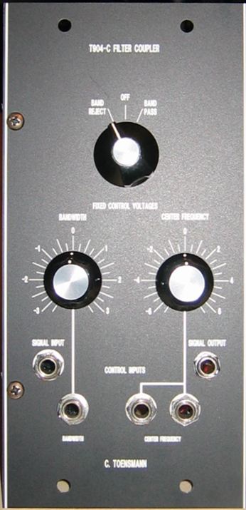
Frontend:
The front panel looks like the ones of the 904a and b - beside the functional differences of course.
It is of double Moog standard size (2 x 2.125"). The functions of the "human interface" (connectors, switch, pots) of the T904C are identical to the original 904C module. Again the voltage values engraved around the FIXED CONTROL VOLTAGE knobs (BANDWITH and CENTER FREQUENCY) are a fake, as the circuit behind it only provides a subset of these voltages (see schema), but the reaction of the module is the same as if the engraved voltages would have been provided at the control voltage connectors.
The function switch determines the signal routing and therefore the band function. The OFF position decouples the 904a and b filter from the coupler to use them stand alone in their basic function.
The 6.3 mm connectors serve as what is engraved above and below them. No level adjustment pots; this task can be done by the 995 attenuator module(s).
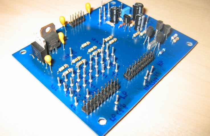
Board of the T904C:
|
|
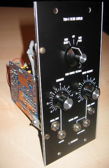
Complete module:
Sound example
- Band reject: A sequence with band width modulation in band reject mode. You can hear only bass and high frequences at one end of the modulation cycle and dominant midrange frequences at the other end.
- Band pass: A sequence with center frequency modulation in band pass mode. You can hear the moving cutoff frequency of the band pass.