T911 Envelope Generator Bank


Introduction

With this module bank my System 55 clone has reached a status of being a stand alone instrument. Three envelope generators combined to a module bank enable the system to be played without further "assistance" of other modular equipment, so this is is an important milestone for the instrument building process. All earlier module tests of my System 55 clone had to be done with additional functions of my Formant modular system, but from now on my System 55 is independent.

The Moog 911 is a standard envelope generator which passes an ADSR sequence, like many other EGs of other manuafacturers also. A gate signal initiates the (A)ttack phase, and the envelope is beeing started. After reaching it's maximum it enters the (D)ecay phase, where the envelope falls down again to a voltage level determined by the (S)ustain level. This voltage level is kept until the gate event terminates. Then the final (R)elease phase is initiated.
The timing of the individual phases and the sustain voltage level is determined by potentiometers on the front panel (see human interface below).

T911 Envelope Generator Bank


Differences to the original

Like for my T902 clone I decided to combine more than one module to a module bank behind one front panel. I decided to combine three ADSRs to one single bank because in a lot of Moog modular systems three ADSRs are configured, together with three VCA (902) modules, one trigger delay and one CV router, all as separate modules of course, to one functional unit. This makes sense, and the way how to use this unit is described in the Moog Modular User's Manual. So here is the next part of this functional unit - the ADSR bank.

Flow of STrigger and envelope CV of the functional unit (taken from Moog Modular Owners Manual):


Another add-on is a 6mm LED which serves as envelope indicator and follows the envelope with its brightness. This is quite useful to get a quick optical overview which ADSR is triggered and (roughly) which kind of onvelope is created.

Complete Module


Click to enlarge

Click to enlarge

Click to enlarge

Click to enlarge

Click to enlarge


Frontend / Human Interface

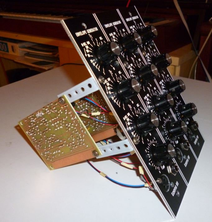
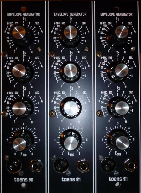
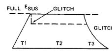
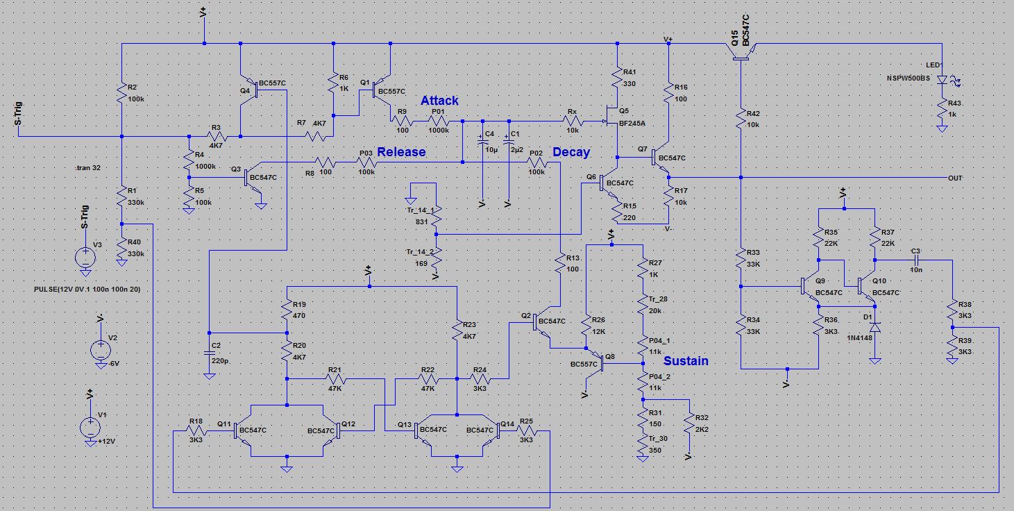
ADSR

The envelope is initiated by a so called "STrigger" event, where a reference voltage within the 911 is shortened to ground (Shorted Trigger). This voltage drop initiates the ADSR process. The reference voltage is provided at the Cinch Jones connector at the lower left of the front panel (see Cinch Jones description below). This connector is usually connected via cable to a device which shortens the reference voltage to ground to trigger the 911 to start with the envelope process. These devices can be a keyboard, a sequencer or other devices which have the task to "play a note".

The envelope starts with an "attack" phase, where the output voltage provided at the 1/4" phone jack at the lower right side of the 911 front panel rises from 0V to 6V in a time which is determined by the T1 pot at the top of the front panel. After the maximum envelope voltage is reached the 911 enters the "decay" phase, where the output voltage goes down again until the "sustain" level is reached. The sustain voltage is set by the fourth pot. The time which is needed to lower the output voltage to sustain level is determined by the second pot on the front panel, T2. This sustain voltage is kept until the STrigger event disappears, e. g. a key is released or a step sequencer stops running.
After the STrigger event has stopped the "release" phase starts to lower the envelope voltage to 0 again. The duration of the release phase is determined by the third pot, T3.
After the release phase is terminated the state of the 911 is "waiting for the next STrigger event".

An LED on the upper right side of the front panel indicates the envelope output voltage by its brightness.

The labelings of the T1, T2 and T3 pots indicate the time a phase lasts, from 2 msecs to 10 secs. This is not really usefull in the msec area as this is barely audible. And the 911 circuit is not the most precise, so the benefit of this labeling is doubtful. But for a rough orientation it's ok.
The labeling of the sustain pot corresponds to the sustain voltage of the output envelope.


Circuit

Schema: Attention: Clicking the schema means acceptance of disclaimer on page bottom! Please refer to the original schematics for more details / component values.


STrig and the Cinch Jones connector

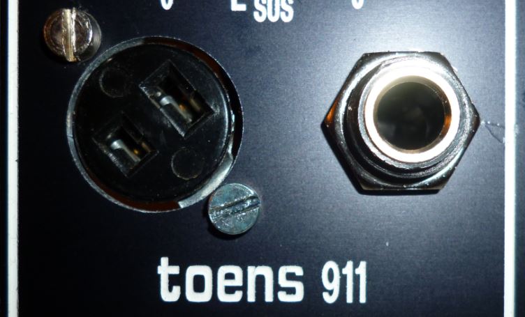
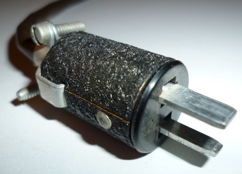
Cinch Jones jack and plug

The gate event of a key beeing pressed on the keyboard or of a step of a sequencer is beeing reached follows a different concept in many older Moog synthesizers, inclusive the modular systems, compared to other synthesizer systems. Other synthesizer manufacturers and modular systems use a so called "gate" event which is physically spoken a binary control voltage of 0V (gate off) and somewhat between 5 to 10V (gate on). This control voltage is not handled separately from other control voltages and can be used for other purposes than note playing also.
The Moog concept differs. The "gate" event is not represented as a voltage but as a current sink (STrigger) and therefore should not be mixed with other control voltages. To prevent an accidental connection between signals, control voltages and the STrigger event no 1/4" phone plugs are used to submit the gate event to corresponding modules but so called 2-pole Cinch Jones jacks and plugs. The Cinch Jones jack serves as input for STrigger events, the plug as output (see also 911A trigger delay for more information).
The 2-pole Cinch Jones connector contains two blades of different width on the plug side and the corresponding females on the jack side (see pictures). As the STrigger concept is a current sink, only one pole would be necessary to transmit the event. This is done via the smaller blade. The wider blade works only as ground reference for the connected modules, not as shield like in phone plugs.


Circuit description

The STrig event causes a voltage drop at the STrig node of the circuit. This node is pulled up to 12V via R2. The voltage drop opens the PNP transistor Q1, and the capacitors C4 and C1 are loaded via the "Attack" pot P01. The capacitor voltage is buffered by the FET Q5 and the NPN transistors Q6 and Q7. The multiturn Tr_14 serves as zero output adjustment. The output voltage is buffered additionally by R42 and Q15 and displayed by LED1.

After the output voltage reached the maximum envelope voltage (determined by the voltage divider R33 and R34) the reset circuit around Q9 and Q10 resets the left half (Q11, Q12) of the flip flop (Q11 - Q13) by a short pulse via integrator C3. This opens the PNP transistor Q4 and the "zero" voltage of the STrigger event is "overriden" by the collector voltage of Q4, so Q1 closes again and the Attack phase terminates.

The reset of the left half (Q11, Q12) of the flip flop sets the right half (Q12, Q13) and the "Decay" phase is initiated as Q2 opens. The capacitors discharge via the Decay pot and R13 until the "Sustain" voltage level is reached. This voltage is set by R27, Tr_28 (max. Sustain adjust), the Sustain pot P04 and the min. Sustain adjust around R31, R32 and Tr_30 and is buffered by Q8.

The Sustain level is kept until the STrigger event terminates and the STrigger node of the circuit reaches 12V again. This opens Q3, and the remaining capacity voltage discharges via the "Release" pot P03 and R8. The ADSR sequence is complete.

As one can see the output envelope is not as linear as documented in the original Moog documentation:

Moog documentation

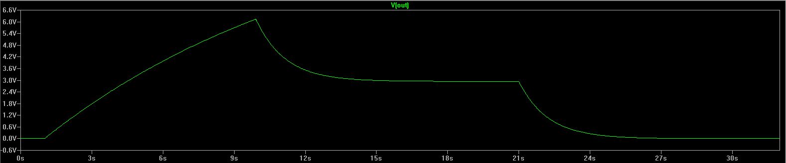
Spice simulation (and reality)

Part replacements

I tried to build my module as close to the original as possible, but I had to do some changes due to actual components I use instead of the originals:

Component changes

Beside the functional addition of the envelope display and the basic changes mentioned above I changed the following component values: The capacitor change was necessary because of the usage of the newer transistor types which have higher betas as the originals. This is only an assumption, and as I don't have an original module to compare I can't prove it. But LTSpice simulation showed that these changes were necessary to let the module work as demanded in the setup and test procedure description of the service manual.

Board of the T911 clone

  • Board dimensions: 75 x 95 mm
  • Upper side: Power supply
    In contrast to the original concept of the Moog modulars I supplied the board with a +/-15V power supply. Voltage regulators on the board convert it to +12V, -6V and -10V. Benefit of this is a higher stability of the power supply.
  • Lower left: flip flop
  • Right: Adjustment
  • Center: all other functions

Click to enlarge

Click to enlarge

Sound example


Additional hints


Please send questions or remarks to:
Carsten Toensmann

Home


Disclaimer:
No warranty for completeness or correctness of technical descriptions, schemas or any information provided on www.analog-monster.de/* pages.
Contents of linked pages are in responsibility of the page owners and analog-monster dissociates from them.
All tracks provided on www.analog-monster.de/* pages is in ownership of www.analog.monster.de (except especially marked) and for private use only. All rights reserved.